
DOWNLOAD
CardBoard gcc v1.2.2 File download
CardBoard GCC v1.2.2 Raw Files (EasyEDA)
CardBoard GCC Info
Ordering Tips
I prefer to order through jlcpcb.com but other board manufacturers may be used as well (have not been tested though)
74VHC126PW,118 must be pre-ordered since JLC does not keep this part in stock
You want the board thickness to be 1.6mm and the finish to be enig (this plates all exposed metal with gold)
Features on the FRONT


figure 1
figure 2


figure 3
figure 4


figure 5
figure 6

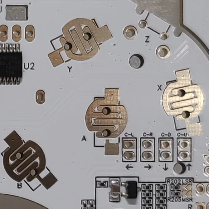
figure 7
figure 8


figure 9
figure 10
SW3 (figure 1)- Analog R customization
- FAR (DIP #1) = Fixed Analog R, the digital press puts out a predetermined analog value. trigger paddle must be soldered/attached to the fixed analog through-hole on the back. To select which value you’d like, close a jumper (figure 3), MSR for Mid-Shield R and LSR for Light Shield R.
- AR (DIP #2) = Analog R, this makes the analog r act as it does on an oem gcc
- DR (DIP #3) = Digital R, the digital press not only puts out a normal digital r signal, but also a full analog value as well. This is useful for when you’re playing with this on a nintendo switch.SW4 (figure 2)- Analog L customization
- FAl (DIP #1) = Fixed Analog L, the digital press puts out a predetermined analog value. trigger paddle must be soldered/attached to the fixed analog through-hole on the back. To select which value you’d like, close a jumper (figure 4), MSl for Mid-Shield l and LSl for Light Shield l.
- Al (DIP #2) = Analog l, this makes the analog r act as it does on an oem gcc
- Dl (DIP #3) = Digital l, the digital press not only puts out a normal digital l signal, but also a full analog value as well. This is useful for when you’re playing with this on a nintendo switch.SW5 (FIGURE 1) - Button Mapping, flip all the switches to the on position if you’d like to have them all function normally. If you’d like to remap one button to another, flip each respective switch to the off position and solder wires from one jumper pad to the other (should look make a criss-cross pattern)
- 1 = B
- 2 = A
- 3 = X
- 4 = Y
- 5 = ZSW7 (figure 2) - enable c-pad, in an effort to reduce the overall cost of a c-pad significantly i have moved most of the necessary components over to the main board, all that will need to be soldered are two 1.1kΩ resistors (through-hole or surface mount) and the four micro switches.
ZL (figure 5), if you have a controller shell that supports a left Z (like the one designed by olympia/sean44104 or eatingproteinpancakes)
- If you’d like ZL to act as just a second z, close jumper j1.
- if you’d like zl to act as a different button, keep jumper j1 open and solder a wire from the ZL Test pad to whatever button you want it to be.T1, T2, and T3 sticks are supported (figure 6). ideally you’d want a t3 stick box with noble potentiometers, but it certainly is possible to solder on T1 and T2 stick boxes to give your old controller a much needed upgrade!
Aftermarket Z is supported (figure 7). Some angled micro switches have mounting pins that are lower than an oem gcc z switch, so instead of having to physically alter the form of the switch, it can just be soldered in normally and effortlessly.
Mouse click A, b, x, and y are supported with mounting holes (figure 8). not only is it possible easily solder on mouse click switches, but it’s also much easier to align the switches with where they need to be!
- link to the switches i useSASI (Sharp Analog Snap-in) is supported (figure 9). The sasi is a custom board designed by sharp02 for a sanwa jlf lever to give it analog capabilities with the use of hall effect sensors and sliding magnet mounts
- for more info on the sasi
- BUY sasi Kit (availability may vary)Tactile D-pad (Figure 10) and start are supported.
- wii classic smd tactile buttons work or you can use theseFight Stick/B0XX Conversion is supported. There are through-holes with solder points on the back for all of the buttons on the controller. This is so they can have a jst connector soldered on and connected to arcade style buttons or joysticks (like the sasi)
- C-stick (figure 8, enable with sw7) and left stick (figure 6, enable by closing left stick jumper pads) have their own solder points for each direction
Features on the BACK

a legend/key for acronyms used throughout the cardboard gcc
a qr code that links to this info page
SW1 (Unlabeled, bottom right) - Left Stick Snapback Filtering
sw2 (Unlabeled, left of Sw1) - PODE* Correction
SW6 (Unlabeled, Bottom Left) - C-Stick SnapBack Filtering and PODE Correction
resistorless cellphone rumble
through-holes for z, l, Fixed Analog l, r, fixed analog r, 3v3 and 5v internal accessory lines
*PODE = Potentiometer oddity degradation effect
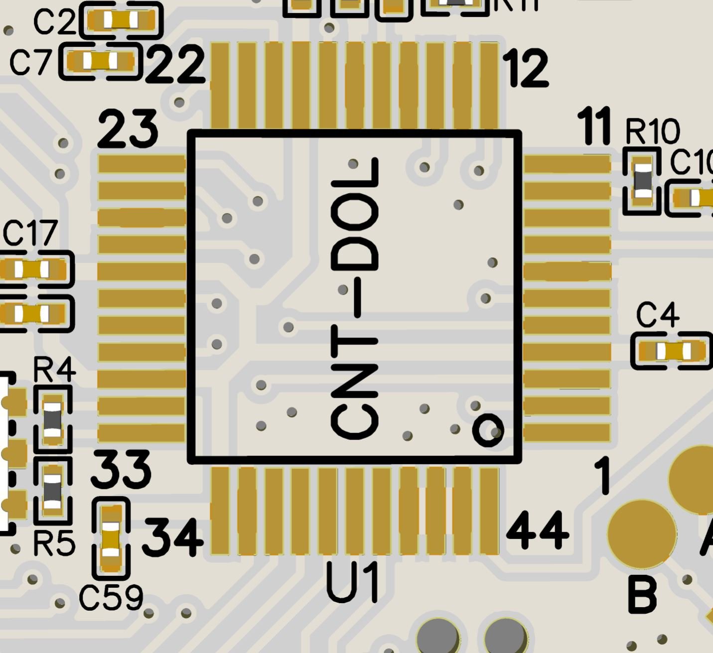
CNT-DOL Pinout
1 - B
2 - A
3 - Rumble I/O
4 - 3.3 Volts
5 - Rumble Brake
6 - Z
7 - GROUND
8 - Digital R
9 - No CONNECT
10 - UNKNOWN
11 - UNKNOWN
12 - Y
13 - GROUND
14 - X
15 - Ground
16 - 3.3 Volts*
17 - Ground
18 - transmit
19 - 3.3 Volts
20 - 3.3 Volts**
21 - No Connect
22 - Digital L
23 - D-Pad Left
24 - D-Pad Up
25 - gnd
26 - D-Pad Right
27 - 3.3 Volts
28 - d-Pad Down
29 - No Connect
30 - start
31 - 3.3 Volts
32 - Clk1
33 - clk2
34 - 3.3 Volts
35 - Ground
36 - Analog L
37 - Left Stick x
38 - Left Stick Y
39 - C-Stick X
40 - C-Stick Y
41 - Ground
42 - Ground
43 - Ground
44 - Analog R
*This line exclusively interacts with the data line and does not connect to the common 3.3 volt line
**This line does not connect to the common 3.3 volt line, it seems to control stick centering in some capacity
OEM GCC Component Info
C17 - 100nf
c18 - 47nf
C19 - 100nf
c21 - 100nf
c22 - 100NF
C23 - 100nf
c24 - 100nf
c25 - 47NF
c59 - 100nf
c60 - 330pf
c61 - 47nf
c62 - 47nf
C1 - 47uf 10v
c2 - 100nf
c3 - 100nf
c4 - 100nf
C6 - 100nf
c7 - 470nf
c8 - 22pf
c10 - 100nf
C11 - 100nf
C12 - 100nf
c13 - 100nf
c14 - 100nf
c15 - 100nf
L1 - 1.8uh
L2 - 1.8uh
L3 - 8.2uh
L4 - 1.8uh
L5 - 1.8uh
Q1 - PNP
Q2 - NPN
Q3 - NPN Epitaxial Planer Type
D1 - 500ma SBD
D3 - 1.1v@1A
Y1 - 4MHZ
F1 - 700 mA 50 V AC 50 V DC
r1 - 10KΩ
r2 - 220Ω
r4 - 1MΩ
r5 - 680Ω
r6 - 220Ω
r7 - 220Ω
r8 - 750Ω
r9 - 100Ω
r10 - 390kΩ
r11 - 220Ω
if you have questions, please don’t hesitate to message me (text or twitter/instagram dms)